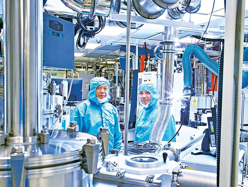
The Applied Materials-NUS Advanced Materials Corporate Laboratory is one of just five corporate labs in NUS and was launched on 25 October last year. This $70 million facility will tap on the expertise of staff from both the NUS Department of Electrical & Computer Engineering and the NUS Department of Chemistry. According to Prof Thean, the collaboration came about because Applied Materials was looking for a university to do “out-of-the-box innovation,” to find completely new ways to engineer material starting from the very fundamentals of chemistry — and NUS embodies all those capabilities. The lab will leverage on NUS’ scientific knowledge in advanced materials built up over more than 20 years. Because the scale of manufacturing these chips is now at the deep-nanometre level, the lab will be doing “precision engineering at the atomic scale”, as Prof Thean describes it. Prof Thean, a prolific inventor with more than 50 US patents in advanced electronics, is the Director of NUS’ new Nanofabrication Facility, E6Nanofab.
“NANO”-MANAGEMENT 101
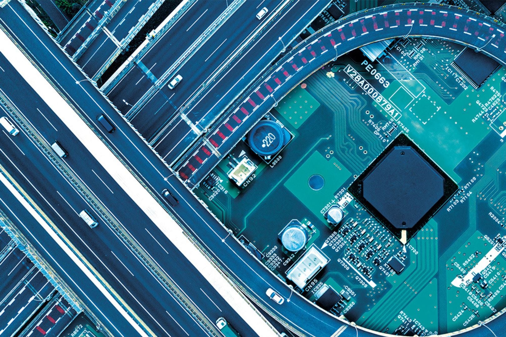
Working at the atomic level has numerous challenges. Among other things, materials behave differently when they are this size. In addition, the materials are so small that their surfaces and interfaces must be carefully engineered for the best performance. In addition, multiple thin nano-scale materials are being stacked together so that they can work as a single entity. All this requires fundamental understanding and innovative research into new materials and their behaviour at an atomic level. If successful, these research projects will lead to smaller and more power-efficient transistors — and thus more powerful computer chips. This can translate to greater storage capacity for USB drives, and faster chips in smartphones, laptops and servers. It will also lead to more computing power to handle the needs of processor-intensive applications like artificial intelligence and storage, processing and analytics.
One of the projects, for example, is looking at a completely new way of etching a semiconductor wafer. Etching is the process during semiconductor manufacturing which uses chemicals to remove layers from the surface of the wafer. As part of this process, some areas have to be masked off so that the unwanted exposed layers can be removed. Currently, etching is done using a process known as photoresist but the new lab is looking at using an atomic layer of carbon to mask areas instead. This would result in a much thinner mask than the current process. “The lab is looking at the ability to deposit the carbon layer as a mask reliably and accurately,” says Prof Thean.
Another research project is looking at improving the wafer fabrication process by using graphene, a type of carbon that is ultra-strong, as a diffusion barrier. In computer chips, barriers are needed to chemically isolate semiconductors from the soft metals used to electrically interconnect them. In a modern computer chip, for example, all the copper used to conduct electricity must be surrounded by a barrier to prevent the copper from diffusing into the surrounding materials. Currently, tantalum nitride, an inorganic chemical compound, is used as the barrier. Graphene, which consists of a single layer of carbon atoms, would result in a much thinner, stronger barrier. “Ultimately, to build the next big technology we will start from the tiniest of parts, and this requires us to innovate at the atomic level for industrial scale,” adds Prof Thean.